

Table of Contents
- What is Switch Bouncing and Debouncing?
- What is Software Debouncing?
- Switch Bouncing Circuit Diagram
- 1. Hardware Debouncing
- └ Components Required
- └ Debounce Circuit Diagram
- └ Working of the Hardware Debounce Circuit
- 2. RC Debounce Circuit
- 3. Debouncing Circuit for Push Button Using Specialised ICs
- Debouncing Methods Comparison
- Common Switch Debouncing Questions Answered
- Explore More Foundational Circuits
What is Switch Bouncing and Debouncing?
When we press a pushbutton, or toggle switch, or a micro switch, two metal parts come into contact to short the supply. But they don’t connect instantly; the metal parts connect and disconnect several times before the actual stable connection is made. The same thing happens while releasing the button. This results in the false triggering or multiple triggering, like the button is pressed multiple times. It's like a bouncing ball from a height, and it keeps bouncing on the surface until it comes to rest.
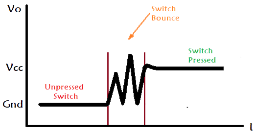
Simply, we can say that switch bouncing is the non-ideal behaviour of any switch that generates multiple transitions of a single input. Switch bouncing is not a major problem when we deal with power circuits, but it causes significant issues in logic or digital circuits. To eliminate this problem, various techniques are implemented using specialised debounce circuit diagrams and components.
What is Software Debouncing?
Debouncing also occurs in software, while programmers add delays to get rid of software debouncing. Adding a delay forces the controller to stop for a particular time period, but adding delays is not a good option in the program, as it pauses the program and increases the processing time. The best way is to use interrupts in the code for software bouncing. Arduino has code to prevent the software from bouncing.
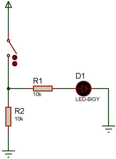
Switch Bouncing Circuit Diagram
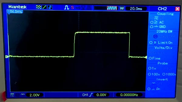
First, we will demonstrate the circuit without the switch debounce.
Each debouncing circuit for push button applications has specific advantages. The Switch bouncing circuit diagram offers simplicity and cost-effectiveness, while hardware-based solutions provide superior performance. Understanding different configurations helps engineers choose the most suitable approach for their specific applications.
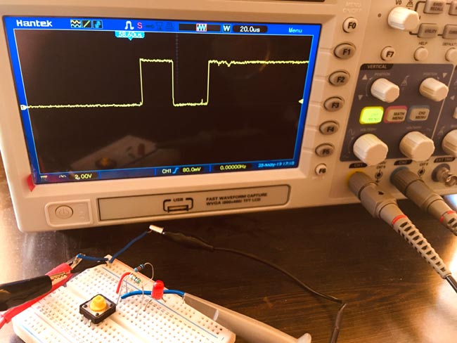
You can also see the waveform in the oscilloscope while push button in bouncing. It shows how much bouncing has occurred during the switching of the pushbutton.
There are three commonly used methods to prevent the circuit from switch bouncing.
- Hardware Debouncing
- RC Debouncing
- Switch Debouncing IC
1. Hardware Debouncing
In the hardware debouncing technique, we use an S-R flip flop to prevent the circuit from switching bounces. This switch bouncing circuit diagram implementation is considered the most reliable debouncing circuit for push button applications, offering superior noise immunity and stable output transitions.
Components Required
- Nand Gate IC 74HC00
- Toggle Switch
- Resistor (10k -2nos.)
- Capacitor (0.1uf)
- LED
- Breadboard
Debounce Circuit Diagram

Working of the Hardware Debounce Circuit
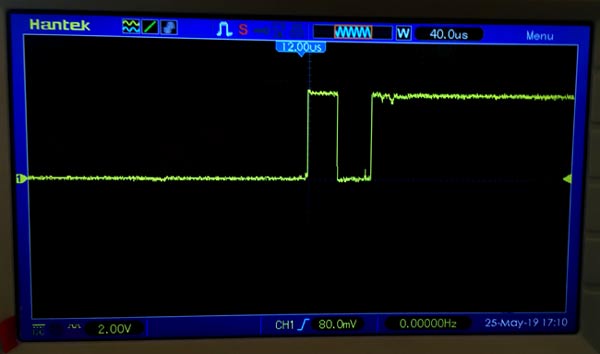
The circuit consists of two NAND gates (74HC00 IC) forming an SR flip-flop. As you can see in the circuit diagram, whenever the toggle switches to the A side, the output logic gets ‘HIGH’. Here, we have used an oscilloscope to detect the bouncing. And, as you can see in the waveform given below, the logic is shifting with a slight curve rather than bouncing. The resistors used in the circuit are pull-up resistors.
Whenever the switch is moving between the contacts to create the bounce, the flip-flop maintains the output because the ‘0’ is fed back from the output of the NAND gates.

2. RC Debounce Circuit
The RC debounce circuit is a resistor-capacitor network to protect from switch bounce and is a popular choice for a simple switch debounce circuit. The capacitor in this filter out the instantaneous changes in the switching signal. The voltage across the capacitor is zero when the switch is in the open state. At first, with the switch in the open state, the capacitor will charge through the R1 and R2 resistors, which creates a stable transition which is ideal for switch bouncing and debouncing.
This simple switch debounce circuit configuration is utilised a lot in both educational and commercial projects. Because of its low parts count and reliable performance, this can easily be adjusted by varying resistor & capacitor values to create variations in timing as described in the above debounce circuit diagram
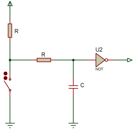
When the switch is closed, the capacitor starts discharging to zero; hence, the voltage at the input terminal of the inverting Schmitt trigger is zero, so the output becomes HIGH.
In the bouncing condition, the capacitor stops the voltage at Vin until it reaches Vcc or Ground.
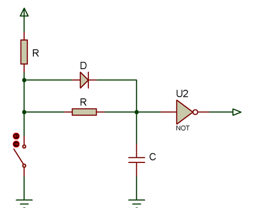
To increase the speed of RC debouncing, we can connect a diode as shown in the image below. Thus, it reduces the charging time of the capacitor.
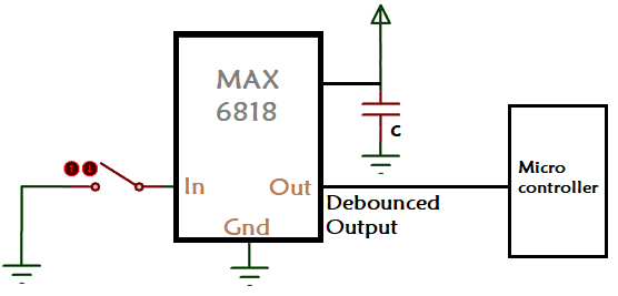
3. Debouncing Circuit for Push Button Using Specialised ICs
There are ICs available in the market for switch debouncing. Some of the debouncing ICs are MAX6816, MC14490, and LS118.
Below is the circuit diagram for switch debouncing using MAX6818.
Debouncing Methods Comparison
Method | Cost | Complexity | Purpose |
|---|---|---|---|
| RC Debounce Circuit | Low ($0.50) | Simple | Basic projects, prototyping |
| Hardware Debouncing | Medium ($1-2) | Moderate | High-speed, reliable applications |
| IC Debouncing | High ($2-5) | Low | Professional, multiple switches |
Common Switch Debouncing Questions Answered
⇥ What is the easiest switch debounce circuit?
The RC debounce circuit is the easiest solution to implement. The RC debounce circuit is simply a resistor-capacitor (RC) network with a Schmitt trigger to block fast voltage changes and provide stable and reliable switching of electronic circuits for us in digital circuits.
⇥ How does an RC debounce circuit work?
In an RC debounce circuit, a capacitor is used to smooth out instant voltage changes caused by switch bouncing. The capacitor charging and discharging will also pass through resistors and will cause the voltage to change smoothly from low to high, which will prevent the relay from triggering multiple times on a digital system.
⇥ What do I need for a debouncing circuit for a push button?
To make a simple debouncing circuit using an RC timer, you will need: resistors (10kΩ), capacitors (0.1µF), AND gates (74HC00) and toggle switches for testing and LEDs (for seeing testing effort). In a more advanced or elaborate solution, debouncing integrated circuits (ICs) like MAX6816 should be used as well.
⇥ What voltage levels are appropriate for using debounce circuits?
Debounce circuits work with any standard logic levels: 3.3V and 5V are standard levels for both digital systems. RC debounce circuits work with TTL (0-5V) and CMOS (0-3.3V/5V) logic families, and hence have a wide popularity among the electronics of the modern day.
⇥ Can switch bouncing ever damage digital circuits?
No, switch bouncing itself never damages circuits. But switches can trigger false state changes, multiple counts, or portray erratic behaviours, all detrimental to proper digital circuits. And this artefact becomes particularly problematic in counters, state machines and interrupt-driven applications.
In conclusion, we've explored how push buttons create switch bouncing effects and demonstrated multiple prevention methods using various switch debouncing circuits. From simple switch debounce circuit implementations using RC networks to advanced hardware solutions, each debounce circuit diagram offers unique advantages for different applications. Understanding these principles is essential for reliable digital circuit design.
Key Takeaways: Switch Bouncing Prevention
- Switch bouncing creates 5-10 false triggers lasting 1-20ms in mechanical switches
- RC debounce circuits offer the simplest solution using basic resistor-capacitor filtering
- Hardware debouncing with flip-flops provides the fastest, most reliable switching performance
- Debouncing circuit for push button applications prevents false counting and system errors
- Specialised ICs like MAX6816 handle multiple switches efficiently in professional designs
- All switch-bouncing circuit diagrams require proper component selection and testing verification
Explore More Foundational Circuits
A mix of practical analog and digital circuits that help clean signals, handle voltage issues, and improve reliability in electronic designs.

Implementing Schmitt Triggers using Op-Amp
We will be designing a simple Schmitt trigger using an Op-Amp. So, in this article, we will discuss where Schmitt triggers are used, how they work, and how to build a Schmitt trigger using an op-amp.

Summing Amplifier or Op Amp Adder Circuit
Today we are going to study one more application of Opamp, which is to add two or more input voltages and the circuit is called Summing amplifier or Opamp Adder.

230V AC Mains Over Voltage Protection Circuit
We are going to build an over voltage protection device with an op-amp, which can detect high voltages and can cut off the input power in a fraction of a second, protecting the device from a high voltage surge.
